
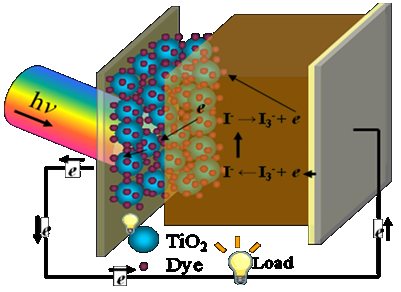
The worldwide fossil energy crisis has brought much attention to the pursuit of alternative energy sources. Solar energy is one of the most abundant and green energy supplies. Dye-sensitized solar cell (DSSC) is a low cost photovoltaic device based on an organic sensitizer attached on a porous metal oxide semiconductor followed by an iodide/tri-iodide contained polymer electrolyte and a counter electrode. Figure 1 shows the schematic illustration of DSSC architect and working function. Electrons in dye molecules are excited by sun light incident through the front window. The excited charges inject into TiO2 anode electrode then go outside circuit and reach counter electrode. The electronic charges are transferred to tri-iodide to yield iodide that reduces dye molecule to its original state.
Different than traditional and expensive Si-based or p-n junction thin film solar cells, DSSC takes advantages of the high surface area of mesoporous thin films for harboring the light sensitizers.2 Porous titanium dioxide has been demonstrated to be the most efficient material to incorporate with dye molecules. This project focuses on the fabrication through a sol-gel method with the assistance of polymer templates as structure directing agents to generate porous structures with pore size ranging from a few to hundreds nanometers. The integrated solar cells are subject to characterization of the photo-electrical energy conversion efficiency using a semiconducting measurement system with an illumination of sun light simulator.
Another goal of this project is the development of new polymer ionic electrolytes with high conductivity and excellent mechanical strength. The polymer gel electrolytes are qualified to fabricate solid state DSSCs and superior to liquid electrolytes in leakage concern. The highly stable and reliable polymer electrolyte potentially improves solar cell quality.
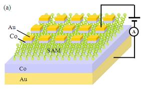
SAM-Based Molecular Junction DevicesA simple, inexpensive and rapid prototyping method to construct thin film molecular spintronic devices has been developed. The goal is to study the spin-polarized current tunneling through a self-assembled monolayer (SAM) spacer. This unique multilayer device provides an excellent test bed to investigating the spintronic behavior at the molecular level. It is of great significance for fundamental understandings of ballistic electron transport through nanoscale thickness molecular monolayers. Metal/SAM/metal junction array can be established via contact printing, a promising way to hybridize an inorganic metal layer onto an organic molecular layer without degrading the organic molecules. Magnetoresistance effects will be examined under external applied magnetic fields and variable temperatures.
Molecule and magnetic metal-based sandwich junctions can be used for molecular memory and magnetic tunneling junction data storage. For example, a sandwich structure consisting of Au/Co/SAM/Co/Au is displayed in the Figure 2. The reactive layer is an alkanedithiol with the functional group SH at both ends of the molecule. The bottom double layer was deposited on Si with a very thin underlying Ti adhesion layer (2-5 nm) by e-beam evaporation. The coated substrate was immersed into a dilute alkanedithiol solution for 24 hours. Molecules close packed themselves into a self-assembled monolayer on metal Co thin film. The other head groups of the molecules are now facing out and ready to bond to another layer of metal. The top double-layer metal array can be transferred onto the SAM from a pre-coated elastomeric PDMS stamp with desired features. Various metals and molecules may be incorporated in different combinations to support interesting applications such as chemical sensors and biomaterial detectors.
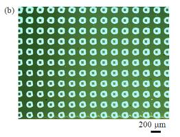
Conventional photolithography has been employed until now as a method of reproducing micro-patterns through complicated steps such as exposure, development and etching. However, it is not suited for materials with a low heat resistance and low mechanical resistance such as single layer molecules, cells, DNA and enzymes. Contact printing, so called soft lithography, provides an alternative and efficient method to produce micro patterns through a featured elastomeric polymer stamp.
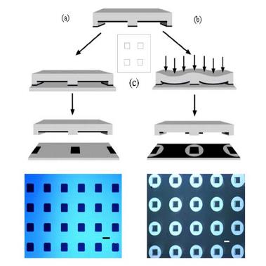
Deformation can occur upon contact with the substrate due to the flexibility of the elastomeric stamp. Figure 3 shows the two different processes of deformed and non-deformed contact printing, rendering totally distinct pattern results.
The utilization of stamp deformation can not only replicate patterns on the stamp but also produce new patterns unavailable on the stamp. To produce new desired patterns, stamp dimension has to be designed in accordance with the theoretical calculations. Pitch size, height, distance as well as the applied pressure take critical rules in the performance of deformation. Multiple-step deformed contact printing results in smaller pattern size compared to the original feature size on stamp. Therefore, nanoscale patterns and structures are expected to be realized through the deformation.
Despite the deformation, contact printing enables printing of patterned molecular monolayers on a large scale from square microns up to square millimeters without producing electrical shorts between the metallic contacts. This opens the possibility to characterize the electrical behavior of metal-molecule-metal junctions on a large ensemble, potentially used for practical applications such as data storage, chemical sensor, and biomaterial detection.
Coming soon!